System News:
hardware-linearisation 19.990 Euro
Datasheet
Our High-Speed AFM offers a wide Spectrum of Measurement Methods:
High resolution Contact mode
High resolution Dynamic mode
Current-AFM Mode
Lateral force mode
Lateral force imaging
Force Spectroscopy
Kelvin Probe Force Microscopy
Kelvin Probe Force Microscopy
Magnetic Force Microscopy (2nd trace imaging)
Magnetic Force Microscopy
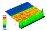
Topography (left) and MFM Amplitude (right) images of a Bruker reference sample for MFM. Image Size: 1.5 µm x 1.5 µm.
Topography (left) and MFM Phase (right) images of a Bruker reference sample for MFM. Image size: 40 �m x 40 �m.
Electrical Force Microscopy
Electrical Force Microscopy
EFM Mode (Single trace)
Topography FWD
EFM Signal 1st Harmonic FWD
EFM Signal 2nd Harmonic FWD
EFM Mode (Dual trace = Lift Mode)
Topography FWD
2nd Trace Amplitude FWD
2nd Trace Phase FWD
Nano-Lithography with script-language
Elastic Force Microscopy (Force Modulation Mode)
Optional Features
Vibration isolation table under the microscopeLow noise laser module
Camera Specification
Camera Sensor
2592 x 1944 Pixel (5 MPixel)
Camera Sensor Type
CMOS color
Optical Sensor Dimensions
3.620 mm x 2.720 mm (4.53 mm diagonal)
Pixel Size
1.4 µm
Optical Resolution
< 4 µm
Pixel Resolution
500 nm
Field of View
1.3 mm x 1 mm
Filter
blue filter (for DNC laser suppression)
Sensor Interface and Power Supply
USB 2.0
controller for the fast Approach of Tip and Sample
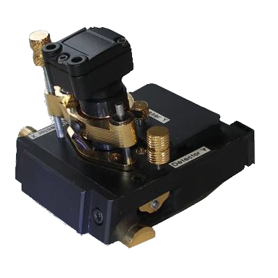
Image of the AFM head with the compact Top View camera design
and Sample Illumination
AFM-Head including a Top View USB-Camera and Sample Illumination
The USB-camera combines a 5 MPixel CMOS sensor and high resolution optics with low
a magnification. The resulting large field of view enables quick location of the area of
interest. An optical resolution below 4 µm ensures the visibility of small
structures. An implemented filter reduces the intensity of the back reflection of the
red DNC laser. Therefore, high quality images during scanning in non-contact mode is
possible.
Camera Images
Camera image of a the AFM cantilever above a TGF11 calibration grating with 10 µm pitch illuminated by a white LED.
Camera image of a calibration glass slide with 10 µm scale bar illuminated by a white LED.
Image of self-assembled 850 nm polystyrene spheres coated with silver. These grating-like structures refract visible light in different colors. The black spots correspond to silver islands. Image of self-assembled layers of 350 nm polystyrene spheres coated with silver. Different layers (mono- or bilayer) give rise to different colors. The black spots consist of silver islands.
Image of a µmash NSC15 cantilever. The tip apex (pointing towards the camera) is shining red. Image of a gold coated high-speed SU8 cantilever.
Illuminated by a white LED.
Illuminated by a green LED.
Illuminated by both, white and green LED.
Image of a monolayer of hexagonal packed self-assembled 850 nm polystyrene spheres coated with silver. These grating-like structures refract visible light in different colors depending on the layer orientation and the wavelength of the incident light.


 Molecular Vista