Parameters and Special Features:
- Multi-Kelvin Controller with Network Connection
- Work Function resolution: < 1 meV with 1.4 mm tip diameter on metals
- up to 9 integrated Kelvin Probe Heads
- Dead Zone Definition for smaller Wafer Diameters and Wafer Parts
- Motorized Approach and Head Selection
- Rotation axis for the Wafer with integrated Angle Encoder for Position Sensing
- Rotation Angle Sensing Resolution: 1 mdeg
- Motorized X-Motion over 100 mm with 50 μm Positioning Accuracy
- Scan Range Overlap between the Sensors
- Integrated Calibration Procedures for
- Tip Length
- Work Function
- Phase Offset
- Automated Data Acquisition Procedures for
- Full Wafer Images
- Small Wafer Images
- Half-Wafers
- Quarter-Wafers
- Lines
- Points
- Humidity and Temperature sensor (USB)
- Integrated Reference (HOPG or Au)
- Scripting language for the programming of user defined measurements
- Integrated Faraday shield
- Gold plated steel frame
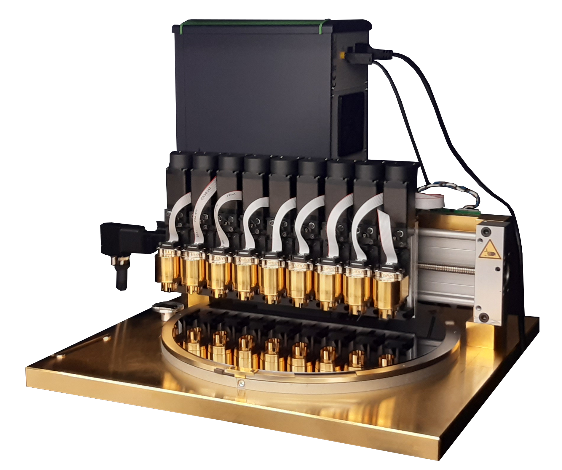
This Scanning Kelvin Probe System moves 9 individual KP heads in vertical direction in
order to realize an motorized approach between the KP Probe and the
Sample. The Samples are clamped on a rotating chuck,
while a rail moves all 9 heads simultaneously in X-direction along the
radius of the wafer and thus allowing a scan range overlap between the heads.
Software based length and work function calibration procedures make sure that
the overlapping work function scans result in a uniform work function image
of the total wafer area.
Automized procedures allow for imaging of full, half or quarter wafers
as well as wafers with smaller diameters.
Manual of the MultiKelvin
(PDF, 1.1 MB) |
 |

 Molecular Vista