





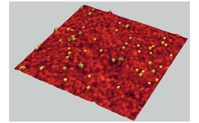


30 nm Gold clusters with functional coatings adsorbed on a
gold surface Image size: 2 µm x 2 µm x 38 nm Sample of courtesy by:
Dr. Plutowski, University of Karlsruhe, Institute of Chemistry.
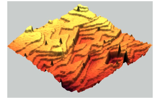


Hydrogen passivated Si(111)-surface with atomic steps
Image size: 1 µm x 1 µm x 4 nm Sample of courtesy by:
Dr. Heike Angermann, HMI Berlin
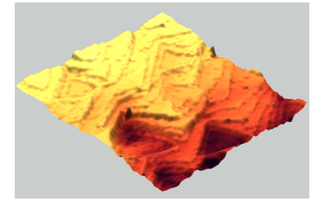


Hydrogen passivated Si(111)-surface with atomic steps
Image size: 1 µm x 1 µm x 4 nm Sample of courtesy by:
Dr. Heike Angermann, HMI Berlin
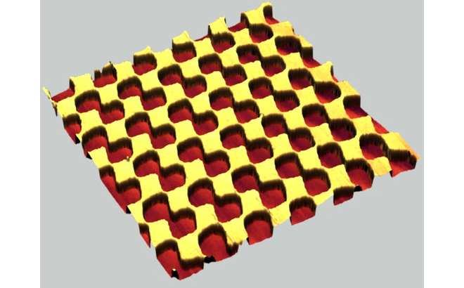


Topography of UMG03/Pt grating
Image size: 10 µm x 10 µm x 120 nm
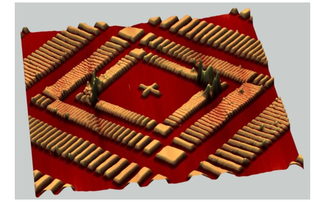


Metal grating produced by electron beam lithography
Image size: 10 µm x 10 µm x 63 nm
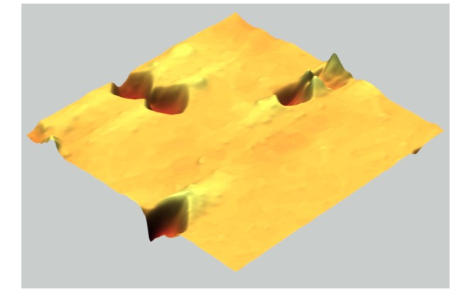


Wet polished stainless steel surface
Image size: 5 µm x 5 µm x 334 nm
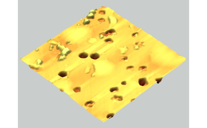


Wet polished stainless steel surface
Image size: 10 µm x 10 µm x 594 nm
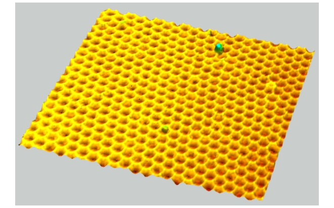


Topography of Porous Aluminum
Image size: 2 µm x 2 µm x 110 nm Sample of courtesy by:
Mr. Ostendorp, University of Münster
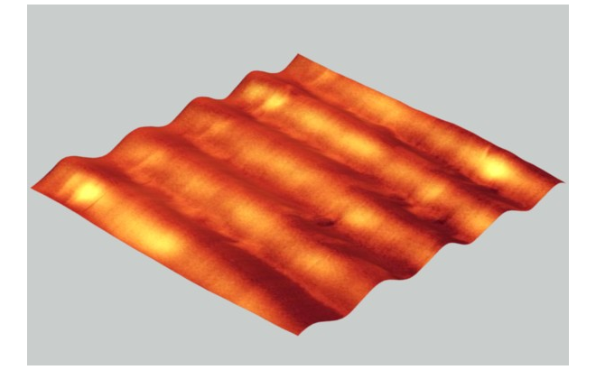


Polymer surface structured with a dual beam laser technique
Image size: 3 µm x 3 µm x 142 nm Sample of courtesy by:
Prof. Pietsch, University of Siegen
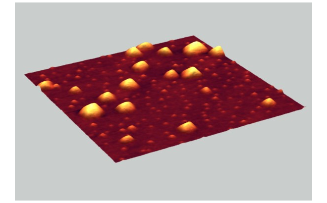


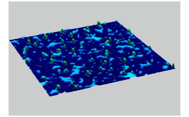
Semiconductive clusters on Si
Ni cluster on a HOPG surface
Image size: 1 µm x 1 µm x 26 nm


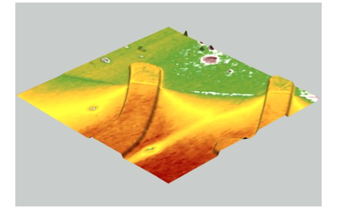
Gold layer on Si(100)
after removal of a plastic foil as cover layer
Image size: 5 µm x 5 µm x 86 nm


KPFM image at the edge of an Al dot with 100 µm diameter
on glass Cantilever: NSC18/TiPt (MikroMasch) KPFM resolution:
approx. 15 mV rms
Image size: 30 µm x 30 µm x 64 nm
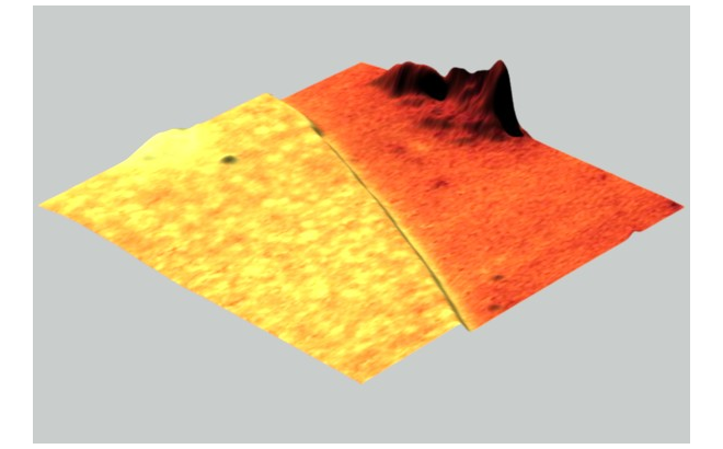


KPFM image of a Au finger electrode on top of an Al
dot on glass Cantilever: NSC18/TiPt (MikroMasch)
KPFM resolution: approx. 15 mV rms
Image size: 30 µm x 30 µm x 64 nm
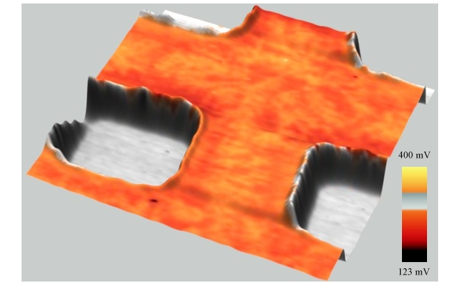


KPFM on a structured Au-layer on a Pt substrate
detected at 240 kHz with ultra-short cantilevers
KPFM resolution: <4mV rms
Image size: 10 µm x 10 µm x 64 nm
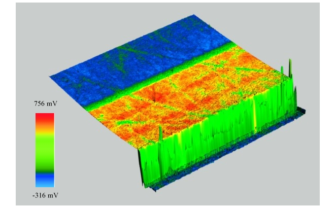


KPFM contrast as color information projected on the topography
as height information of a cross-section of B-doped Si-Wafer
with P- and B-doped Si-Layers
Image size: 20 µm x 20 µm x 178 nm
Sample of courtesy by: H. Schmid (FZ Rossendorf), A. M�ller (SGS Fresenius), Dresden
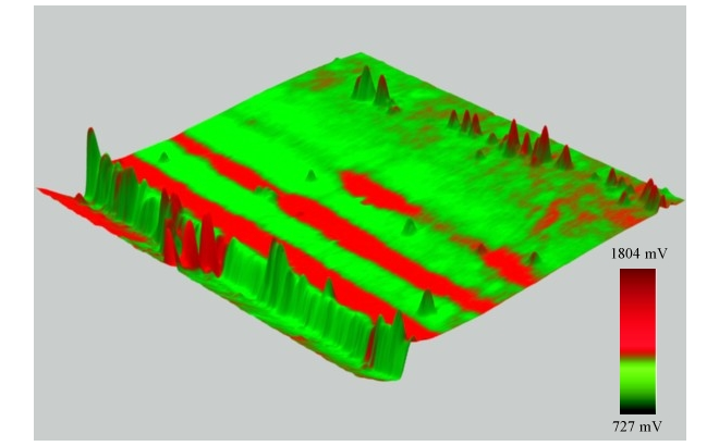


KPFM contrast as color information projected on the topography
as height information of a cross-section of P-doped Si-Wafer with
B-doped Si-Epilayers Image size: 20 µm x 20 µm x 186 nm Sample of courtesy
by: H. Schmid (FZ Rossendorf), A. M�ller (SGS Fresenius), Dresden
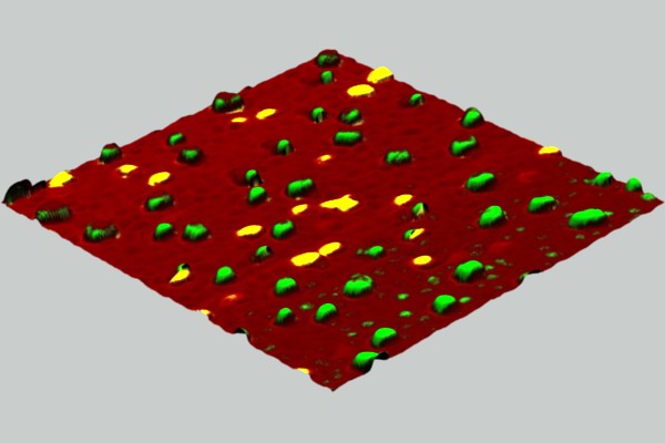


Gold surface with organic contamination
Phase contrast as color information projected
on the simultaneously acquired topography
of organic contaminations on sputtered gold on glass
Image size: 1 µm x 1 µm x 12 nm
Phase range: -28° to 36°
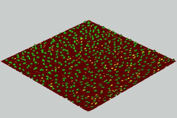


Phase contrast as color information projected on the simultaneously acquired topography
of organic contaminations on sputtered gold on glass
Image size: 1 µm x 1 µm x 9 nm
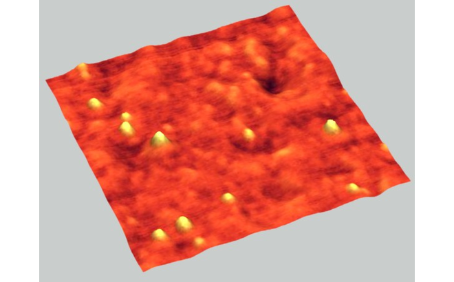


Polymer film with embedded gold clusters
Phase contrast of Au-particles inside polymer sheet
Image size: 500nm x 500nm x 7nm
Sample of courtesy by: M. Gladitz, TITK Rudolstadt