|
Raman Mapping of CNT Bundles on a Silver/Glass Substrate
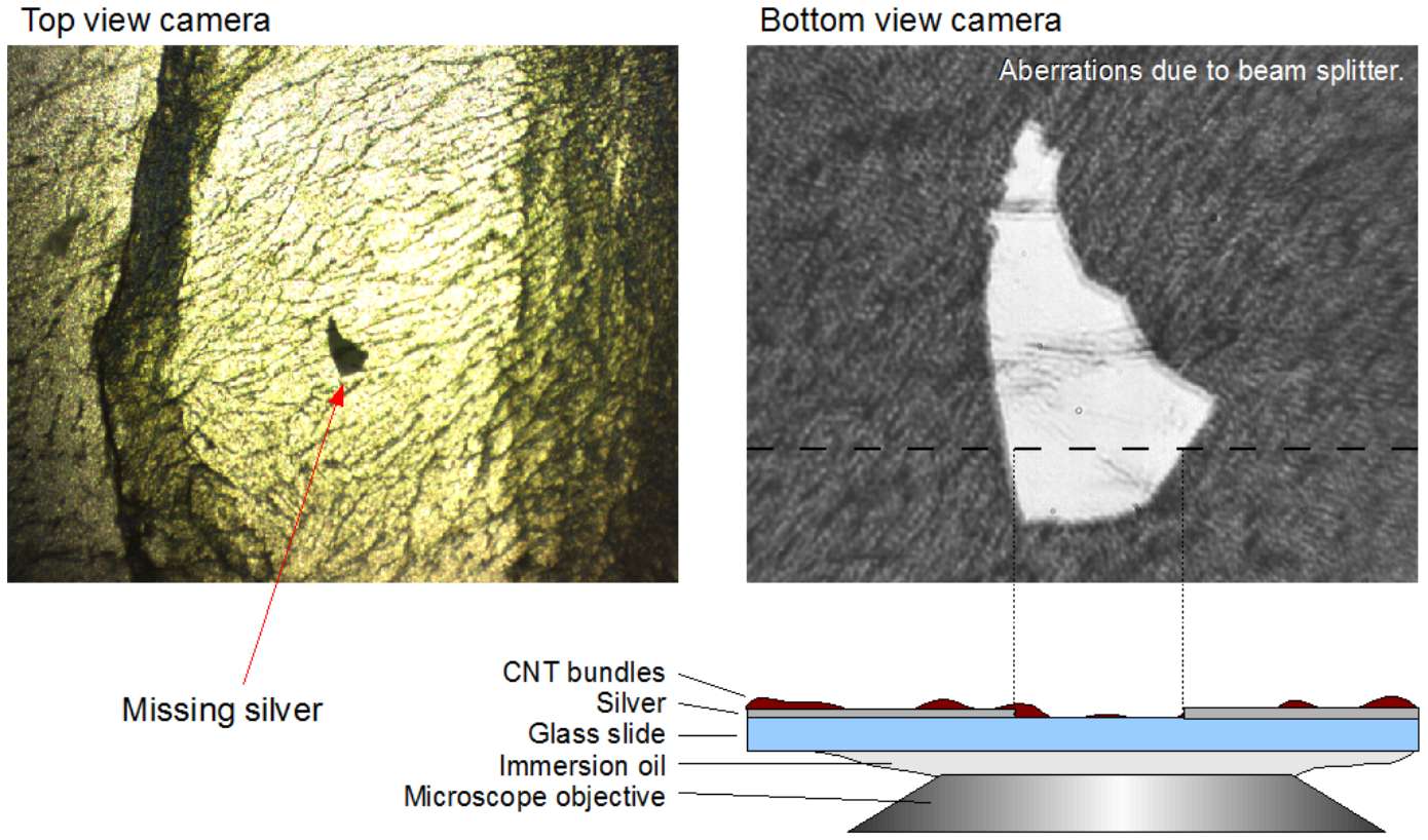
The sample consists of a glass substrate with a thin silver coating. An island-like part of the silver layer was removed and the sample was drop-coated with bundles of (6,5) semiconducting carbon nanotubes (CNTs). The images of the sample on the left are obtained by the top (left) and the bottom (right) objective of the VistaScope. Additionally a sketch of the sample layer structure is shown below the bottom view image.
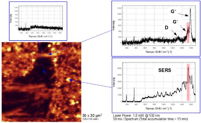
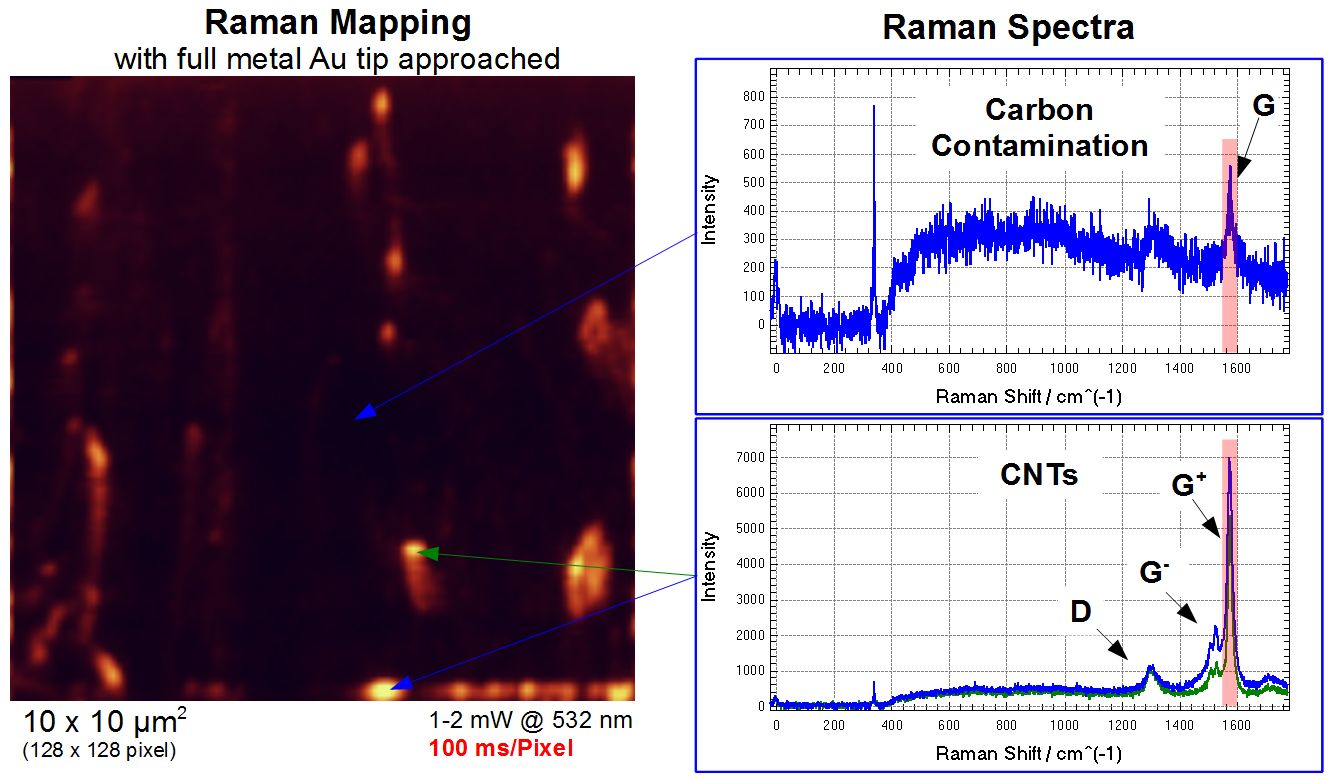
The Raman map on the left shows the chemical information of the sample structure shown above (see also
Applications > Confocal Imaging). The intensity of the G- peak of the CNTs is dispayed as color code in the map. Additionally, some representative Raman spectra are shown. The G- peak is highlighted in red in the spectra. Some very localized spots of the sample show a clear indication of surface enhanced Raman scattering (SERS) due to the rough silver layer below the CNTs.
During mapping, the sample is scanned. At each pixel (128 x 128) one Raman spectrum is captured. The acquire time for each spectrum is 50 ms. A 532 nm diode pumped solid state laser with an optical output power of 1 mW to 2 mW (at the sample) was focused on the sample via the bottom objective.
The image represents a sample scanning size of 30 µm x 30 µm
|
|
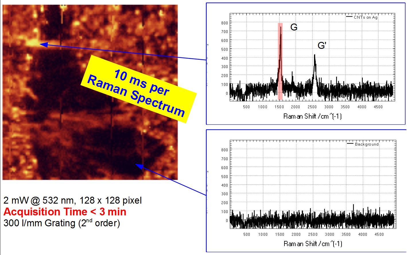
Wide Range Raman Mapping
In order to increase the spectroscopic range of a single spectrum even further, the same sample was scanned with a different Raman spectrometer setting. A spectral window of about 5000 wavenumbers was collected. Therefore, the first and the second order of G peak of the CNTs is well resolved. At the expense of the resolution, the exposure time for each spectrum could be reduced to 10 ms. The total acquisition time of a 128 pixel x 128 pixel image is therefore less than 3 minutes.
The image size is 30 µm x 30 µm.
|

 Molecular Vista